
Photonic Payloads for Next Generation 5G Satellite Networks
V. Polo, M.A. Piqueras, J. Martí, DAS Photonics, Valencia, Spain
IEEE Future Networks Tech Focus, Volume 3, Issue 3, November 2019
Abstract
This paper describes photonic payloads for communication satellites employing microwave-photonics including first in-orbit demonstrations. Due to the characteristics of photonics, such as high flexibility and broad bandwidth, payloads can be designed achieving a significant size, weight and power (SWaP) reduction regarding traditional RF technologies. This combined with the intrinsic low transmission losses and latencies of photonic components and optical fibers make photonics an ideal technology for next generation fiber-in-the-space network architectures for providing 5G global coverage.
1. Introduction
5G networks and technologies are foreseen as the paradigm to satisfy the ever-increasing demand of access to digital content, driven by Internet access, video-on-demand, mobile communications and more recently, by IoT (Internet of Things). Among the different network infrastructures, the only one able to provide truly global operation, seamless access and universal coverage are satellite-based networks, either by themselves or as an extension of terrestrial networks. Until recently, satellite infrastructures were based in geostationary orbit (GEO) satellites with very wide coverage and broadband capabilities. However, their complexity has significantly increased as flexible multi-beam architectures are needed in order to be able to satisfy the new requirements of users and applications globally. Being particularly challenging is the provision of services requiring latencies in the order of ms (milliseconds), and therefore their cost. A possible solution to this limitation are satellite mega-constellations operating at medium/low-Earth orbits (MEO/LEO), making use of GEO satellites as gateways [1], which are much more flexible, potentially cheaper and with latencies between 10 to 50 ms, compliant with 5G requirements [2]. This complex network architecture, combining GEO coverage and high-throughput with the flexibility and low-latency of LEO/MEO constellations all interconnected through RF and Optical inter-Satellite links (ISL), pushes the traditional RF and digital technologies to unprecedent performance, SWaP and cost-effectiveness requirement levels, well beyond the today’s affordable solutions, leading to satellite manufacturers to rethink how satellites have to be built.
Photonics has emerged as an enabling technology to facilitate the implementation and deployment of such next-generation satellite network infrastructures leveraging the tremendous evolution experienced in the terrestrial domain, due to the ability of photonics to handle high data rates and RF bandwidth and its potential for large integration and mass reduction in applications such as multiple local-oscillator distribution, antenna beamforming or multi-frequency conversion at very high frequencies, which are critical in this scenario, especially when the optical fibre is considered in the payload design substituting waveguides or coaxial cables [3-5].
2. Photonic SATCOM architectures
Figure 1 shows the sketch of a fully photonic analogue SATCOM payload. It is comprised by several key building blocks that process the incoming RF signals from the input section of the payload to the output antennas. First, the input RF signal is downconverted using broadband photonic multiple frequency converters (PMFC) which are fed by multiple LO signals coming from a photonics frequency generation unit (PFGU) [6,7] where N LO signals are externally modulated using N CW lasers and E/O modulators, whose output is multiplexed using an optical multiplexer and fed to the PMFC units. An optical switching matrix is used to route the signals from the PMFCs to the appropriate output port. Banks of optical filters could be placed after the routing matrix either as wavelength demultiplexers or as RF-photonic channel filters. At the output of each filter, the signals are converted back to the RF domain using an Opto-electronic converter (O/E), amplified and fed to the output antenna.
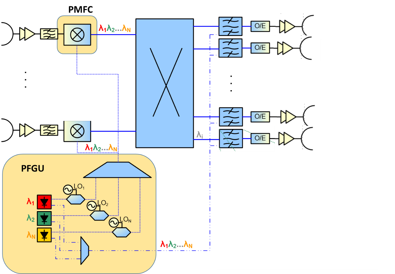
Figure 1. Photonic analogue payload architecture including a multi-frequency generation unit (PFGU), optical distribution system, photonic multiple frequency conversion units (PMFC) an optical switching matrix, photonic filters and Opto-electronic converters (O/E).
Figure 2 shows the sketch of a fully photonic digital SATCOM payload, in which the capability to satisfy the requirements imposed by functionalities such as beam forming and switching, pushes significantly the digital signal processing capabilities to higher data rates. This has a direct impact on the ADC design as conversion bandwidth is limited and must be traded off with resolution. In order to overcome the limitations of the electronics/ADCs, different photonic structures have been analysed [8-11]. The incoming RF signals are directly sampled by using a Photonic ADC scheme, which allows the simultaneous sampling of a broadband spectrum, for example from 500 MHz to 40 GHz. The fundamental concept was demonstrated with 60 dBc SFDR at Ka band in an ESA research program [12], and further enhanced and demonstrated in Ka band within the FP7 project PHASER [13]. When the input signals are digitized, signal processing such as beamforming, equalisation or pre-emphasis can be made in an on-board digital processor. Once the signals are processed in the digital domain, they are then converted back to the optical domain through a Photonic DAC and then routing is performed directly in the optical domain, potentially with high-port count and fast switching speed (in the ns range).
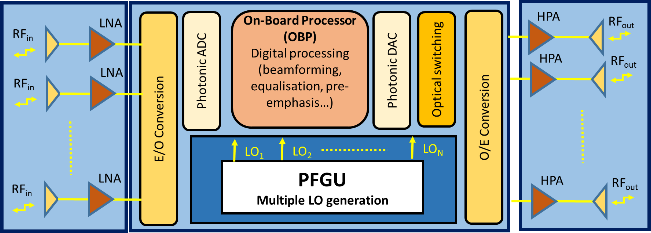
Figure 2. Photonic digital payload architecture including photonic ADC, DAC and Beamforming functionalities.
3. Experimental validation of Key-Building blocks
Recent developments have resulted in the design, fabrication, qualification and in orbit validation of advanced microwave-photonic building-blocks, such as frequency generation and distribution units (including optical amplifiers), Ka/Q/V-band photonic-microwave downconverters and broadband photoreceivers. At a lower TRL, the demonstration of broadband tuneable photonic RF filters and beamforming networks with increasing degree of integration or photonic-assisted photonic ADC is paving the way for a fully transparent photonic payload, either for analogue, digital or hybrid architectures. The PFGU has been subject of significant work during the last decade. In [14], a PFGU was investigated and demonstrated up to TRL5. Further work has led to the design, fabrication and in-orbit-demonstration (IoD) of PFGUs combined with photonic mixers [6, 7]. Recently, in project OPTIMA [15], coordinated by AIRBUS Defense and Space, further miniaturisation has been investigated by co-packaging a distributed-feedback (DFB) laser with an external modulator chip, enabling the same functionality within a reduced size PFGU module.
Figure 3 depicts the simplified architecture of a PMFC (Photonic Multi-Frequency Converter) module. This module allows the mixing of multiple LO signals modulated onto optical carriers with an incoming RF signal in Ku/Ka/Q/V bands. The mixing occurs in a broadband optical external modulator and is replicated for all incoming wavelengths and LO frequencies coming from the LO generation unit (PFGU). Therefore, the incoming RF signal is downconverted simultaneously to several output RF frequencies than can be properly routed to the corresponding output antenna. It should be remarked that the broadband nature of the photonics technology used allows to design a frequency agnostic PMFC, limited only by the bandwidth of the external optical modulator used to perform the mixing process. Therefore, it is possible to design a photonic payload architecture in which the PMFC is universal and is interconnected to the other modules through a standard optical interface. The other module interfaces, namely the PFGU and optical receiver, must be adapted to the exact frequency bands of operation.
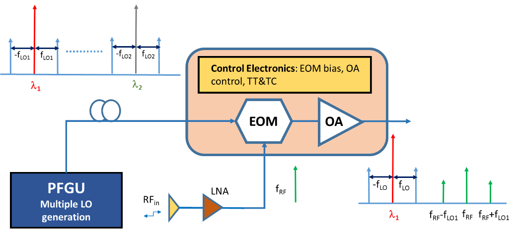
Figure 3 Schematic of photonic multi-frequency converter (PMFC). This concept enables the frequency conversion using multiple LOs. For the sake of simplicity, only 2 LO and 2 wavelengths are used to describe the principle of operation.
Recent work developed by DAS Photonics in collaboration with SSL (a Maxar Technologies company) has led to the demonstration of a Ka-band Flight Demonstration photonic payload aimed for payload solutions for High Throughput Satellites (HTS) systems hosted in a HISPASAT W30-6 GEO Communication satellite [6] and a V/Q Broadband Photonic Converter PFM [7] launched in EUTELSAT 7C in June 2019. The scope of the IoD included qualification level testing per specific satellite environmental requirements, comprising mechanical shock, vibration, TVAC, EMC and EMI tests. At the photonic component level, up-screening and qualification tests was carried out aiming to meet 15 year’s life for GEO orbit and ensuring no failure propagation to the interfacing elements of the satellite. This qualification comprised hermeticity, thermal cycling, mechanical shock, outgassing, Radiation TID and Protons and endurance test for the lot qualification. The PFM was subjected to vibration and TVAC tests. Functional test results have demonstrated the operation of the photonic solution and its suitability for commercial telecom satellites, especially for HTS in which a large optimization of mass, size and power consumption is foreseen respect to a traditional RF implementation. Figure 4 shows a picture of the photonic payload integrated in EUTELSAT 7C and a plot of the Q/V to Ka frequency conversion response at different input RF and LO powers. Figure 5 shows the gain compression and the noise figure of the module.
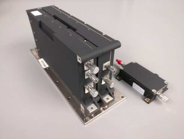
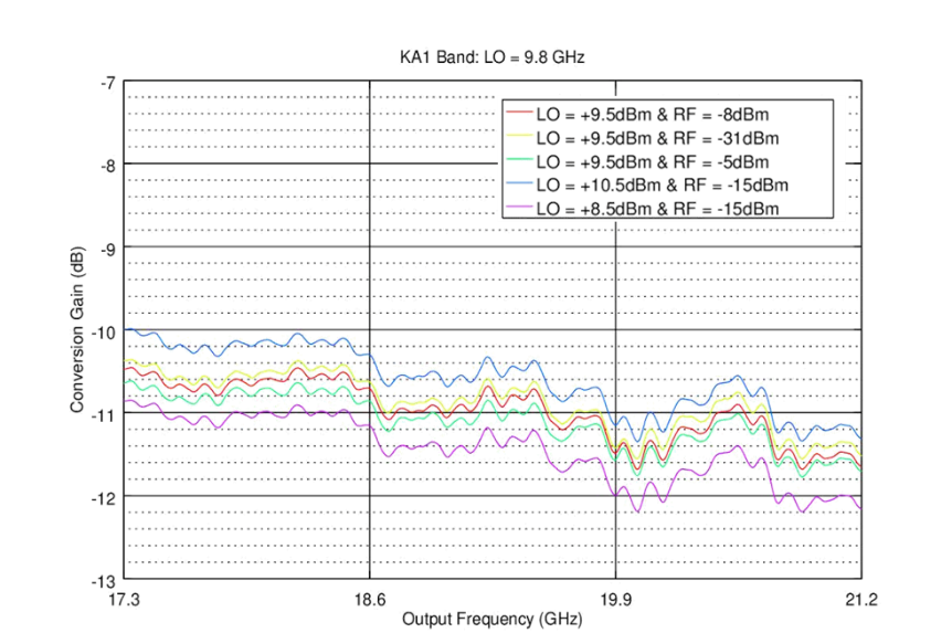
Figure 4: Pictures of the PFM including PFGU and PMFC Q/V band assemblies (left) and conversion gain to Ka at ambient temperature (+25ºC) (right).
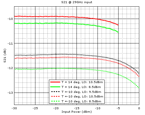
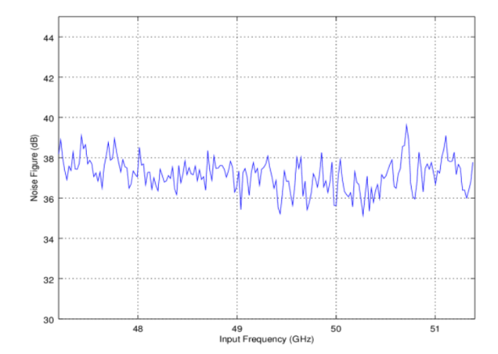
Figure 5. Gain compression vs input RF power at different temperatures (left) and noise figure vs output frequency from V-to-Q band without input LNA (right).
Other important functions to be implemented in a photonic payload is the photonic filtering of RF signals, which exhibit more capabilities than its RF counterpart such as tunability and reconfigurability, which is of tremendous interest for future flexible telecom payloads. Within the ESA TRP contract “Photonic RF Filtering” a filter able to provide central frequency tunability and passband bandwidth adjustability suitable for its use in telecom payloads as both stand-alone RF filter or as a module to be integrated in the future optical telecom payloads was designed and manufactured. The photonic RF filter uses non-linear effects in the fiber to generate spectral regions with gain based on the Brillouin effect [16-17]. In this kind of scheme, a pump signal is injected in the same fiber where the RF signal is present, though in counter-propagating direction. Due to the Stimulated Brillouin Scattering (SBS) effect [18], a gain region is generated some GHz away from the pumping signal. The effect achieved is of active filtering, so the region to be filtered is amplified over the rest of the spectrum. SBS in optical fibers is a particularly interesting phenomenon to perform optical signal processing due to its low threshold power, narrow bandwidth and simple tuning and reconfiguration capabilities. The architecture of the Photonic RF filtering demonstrator [19-20] is shown in Figure 6 (left). The output of a continuous-wave laser is split into two branches. The lower branch is modulated by the RF input signal in an optical phase modulator to generate the Stokes signal. The upper branch is modulated in a Mach-Zehnder modulator to generate the optical pump signal, which counter-propagates then along the Stokes signal to generate Brillouin gain at the desired frequency. The filter has been implemented employing 900 m of highly non-linear fiber which exhibits an SBS frequency shift of 9.7 GHz and an SBS FWHM spectral width of < 24 MHz depending on the optical pump power. The pump modulating signal is generated employing laboratory equipment controlled by a custom graphical user interface (GUI) software. A baseband signal generated from a digital-to-analog converter (DAC) is modulated in an RF synthesizer with IQ modulation to generate a fully reconfigurable electrical pump signal. The filter bandwidth can be adjusted by modifying the number of tones as well as the frequency, amplitude, and phase of the tones of a multitoned baseband signal. The equivalent baseband response of the pump modulating signal can be digitally generated, modified and adjusted. On the other hand, the filter center frequency is adjusted by an RF synthesizer generating local oscillator (LO) frequencies of the center frequency minus the SBS frequency shift. For the SBS frequency shift of 9.7 GHz, the synthesizer should be able to be tuned within 1-3.05 GHz in order the filter gain is within the Ku-band from 10.7 to 12.75 GHz. These frequencies are relatively low and can be addressed by a synthesizer chipset for a filter stand-alone system.
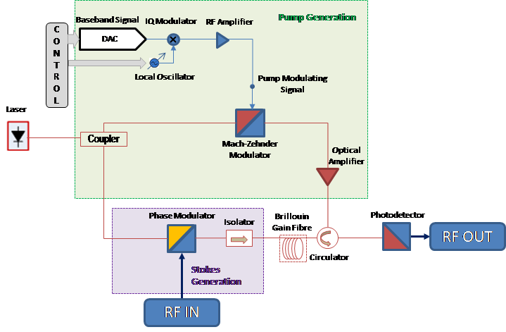
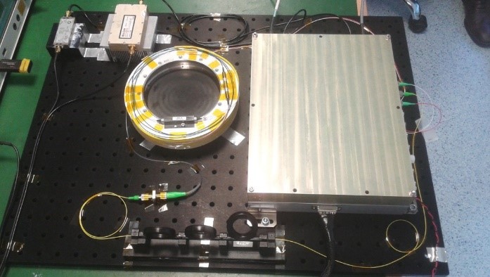
Figure 6. Photonic RF filtering architecture (left) and demonstration (right).
Figure 7 (left) shows the measurements demonstrating the filter center frequency tuning in all the operational frequency range of 2 GHz for the entire Ku-band, from 10.7 to 12.75 GHz. The LO frequency is tuned from 0.907 to 3.007 GHz with 100 MHz steps. Experimentally, passband bandwidths of 36, 54 and 72 MHz where demonstrated. Insertion loss variation of 0.4 dB in-band was obtained, exhibiting better shape factor addressing sharper requirements of the filter insertion loss for higher bandwidth. In cases in which the bandwidth is close to the fundamental Brillouin bandwidth (~19 MHz) the filter shape is dominated by the fundamental response. Out-of-band rejection close to 40 dB is achieved in all the cases. Regarding group delay variation, values close to 2 ns are achieved within the filter bandwidth. Return loss was lower than -10 dB for the frequencies of interest. Figure 7 (right) shows the photonic RF filter response for 72 MHz bandwidth.
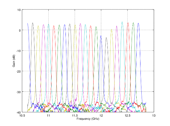
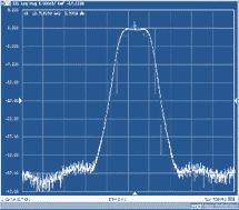
Figure 7. Photonic RF filter gain response tuning within the entire Ku-band (left) and filter response for the 72 MHz passband implementation.
4. Conclusion and Future Prospects
Photonics-enabled payloads can offer an unprecedent degree of flexibility and capacity for next generation satellite infrastructures combining LEO/MEO/GEO constellations interconnected by Optical ISL, required to satisfy the performance requirements of 5G, in particular low latencies thanks to photonics intrinsically low induced delays and switching times. The first in-orbit demonstrations of photonics payloads comprising different building blocks, such as PFGU, PMFC, optical switches and photoreceivers are a reality, demonstrating the maturity and reliability of photonics technologies, building flight heritage and paving the way for future recurrent flight models. In parallel, important advancement in the miniaturization [21-23] and qualification [24, 25] of devices and modules have been achieved. The future generation of the photonic payloads could benefit from the increased degree of miniaturization by using PIC technology, always considering that the increase in the level of integration will not jeopardize the system performance in terms of signal quality, power consumption or reliability. All in all, running programmes such as ESA Scylight HYDRON [26] of EC H2020 projects such as SODAH [27], are relying on photonics technologies as an enabler for next generation satellite communication networks able to provide 5G services.
Acknowledgements
The authors would like to acknowledge the continuous support and guidance from ESA Officers.
References
- O. Khodeli, et al., “Integration of satellites in 5G through LEO constellations”, in Proc. IEEE Glob. Comm. Conf. GLOBECOM, 2017
- N. Wang, et al., “Satellite Communications: what will happen after 5G?, IEEE ComSoc Technology News August 2019 (online)
- J. Anzalchi, P. Inigo, B. Roy, “Application of Photonics in Next Generation Telecommunication Satellites Payloads”, International Conference on Space Optics, ICSO-2014, October 2014, Tenerife, Spain.
- V. Polo and M.A. Piqueras, “Microwave Photonics in Space applications” (Invited), Workshop WS04 “Emerging applications of Microwave Photonics”, European Conference on Optical Communications (ECOC), Rome, 23-27 Sept. 2018
- M. A. Piqueras, “Microwave Photonic Applications for the Next Generation of Telecom Payloads”, International Topical Meeting on Microwave Photonics MWP 2018, 22 - 25 October 2018, Toulouse, France
- M.A. Piqueras, et al., “A Ka-Band Single String Photonic Payload Flight Demonstrator for Broadband High Throughput Satellite Systems and an In Orbit Demonstrator of Optical RF distribution on board satellites”,
- M.A. Piqueras, et al., “A Flight Demonstration Photonic Payload for up to Q/V-Band implemented in a satellite Ka-Band hosted payload aimed at Broadband High Throughput Satellites
- M.A. Piqueras, P. Villalba, J. Puche and J. Martí, "High Performance Photonic ADC for Space and Defence Applications", IEEE COMCAS, Tel-Aviv 2011.
- M.A. Piqueras et al, High-Speed, High Frequency Electro-Photonic ADC for Space enabled routers and flexible antennas”, in Proc. ICSO 2016, 18-21 October, Biarritz, France.
- A. Khilo et al.," Photonic ADC: overcoming the bottleneck of electronic jitter", OPTICS EXPRESS, Vol. 20, No. 4, pp. 4454-4469, 13 February
- Paolo Ghelfi et al., "A fully photonics-based coherent radar system", Nature 507, 341–345, March 2014.
- ESA contract "Electro-Photonic ADC", T516-017MM
- Project FP7-SPACE-2013-1, 607087 “PHASER”.
- ESA contract "Opto-Microwave Wideband Reconfigurable receiver", 4000102535/11/NL/NA
- J. Anzalchi, et. al, “Towards Demonstration of Photonic Payload for Telecom Satellites”, in Proc. ICSO 2018
- X.S. Yao, “Brillouin Selective Sideband Amplification of Microwave Photonic Signals,” IEEE Photon. Technol. Lett., vol. 10, no. 1, pp. 138, January 1998.
- B. Vidal, J.L. Corral, J. Martí, “All-optical WDM multi-tap microwave filter with flat bandpass,” Opt. Express, vol. 14, no. 2, pp. 581-586, January 2006.
- G. Agrawal, Nonlinear fiber optics, 5th ed., Academic Press, 2012.
- ESA TRP contract “Photonic RF Filtering”.
- M. A. Piqueras, et al., “Tunable and reconfigurable photonic RF filtering for Flexible Payloads”, in Proc. ICSO 2016, 18-21 October, Biarritz, France
- F. van Dijk et al, “Integrated InP Heterodyne Millimeter Wave Transmitter, IEEE Photon. Technol. Lett, 2014
- Micro-Opto Electronic Oscillator up to 40GHz based on LiNbO3 (OEwaves) https://oewaves.com/hi-q-oeo
- FP7 Project 607401 “BEACON” http://www.space-beacon.eu/
- H. Meier, “High Power Photoreceivers forHigh Dynamic Range –High Frequency Photonic RF Links”,
ESA SATCOM final presentation days –ESA-ESTEC, 2019 - A. M. Joshi, S. Datta, “Space qualification of InGaAs photodiodes and photoreceivers”, in Proc. SPIE 10641, Sensors and Systems for Space Applications XI, 2 May 2018.
- https://artes.esa.int/funding/high-throughput-optical-network-hydron-scylight-sl021
- https://www.sodahconstellation.eu/
 Dr Valentín Polo obtained the Ingeniero de Telecomunicaciones (MsC) and Doctor Ingeniero de Telecomunicaciones (PhD) degrees by the Universidad Politécnica de Valencia (UPV) in 1997 and 2003, respectively. Since 1997 until 2008, he worked at the Valencia Nanophotonics Technology Center at UPV, engaged in research in microwave photonics for broadband access networks. In May 2008, he moved to AIMPLAS – Polymers Technology Centre as Head of International Projects. In May 2015, he became Projects Director at DAS Photonics (http://www.dasphotonics.com). He has co-authored more than 120 papers in peer-reviewed journals and conferences in the fields of Microwave Photonics and Broadband Access Networks.
Miguel A. Piqueras received the Telecommunication Engineer and PhD degree from the Universitat Politècnica de Valencia, Spain. After five year involved in R&D activities in the Nanophotonic Technology Center (NTC), in 2006 he joined the spin-off company DAS Photonics, participating from its incubation process up to the present, now as Chief of Technology Officer. He coordinates the technical activities of the company and leads different projects in photonic integrated circuits and Microwave Photonic systems for Space and Defence applications. In parallel, he works as external expert for the European Commission.
 Prof. Javier Martí received the Ingeniero de Telecomunicación degree from the Universitat Politecnica de Catalunya (Spain) and the Doctor Ingeniero de Telecomunicación degree (Ph.D.) from the Universidad Politécnica de Valencia, (UPVLC) Spain. Since 2000 he holds a Full-Professor position at the Telecommunication Engineering Faculty in UPVLC. He is Director of the Nanophotonics Technology Centre (NTC), that includes a rapid-prototyping silicon photonics facility, in which several research activities in areas as metamaterials and plasmonics, photonic integrated devices, microwave photonics and integration of high-speed wireless-optical networks. In 2005 he founded DAS Photonics, which is pioneering the supply of advanced photonics-based solutions for Space and Electronic Warfare markets.
He has co-authored over 20 patents and more than 360 papers in refereed international technical journals in the fields of opto-microwave systems and technologies, Silicon photonics circuits and high-speed wireless-optical communications.
He has led many national and international research projects focused on photonic technology and systems and has acted the co-ordinator of many industrial consortia in the European Framework Programs (from FP5 up to FP7). He was a founder of ETP Photonics21, member of its Board of Stakeholders since the foundation as well as member of the Connect Advisory Forum at EU DG Connect.
Editor: Rod Waterhouse

Rod Waterhouse received his BEng, MS, and PhD in Electrical Engineering from the University of Queensland, Australia, in 1987, 1989 and 1994, respectively. In 1994 he joined RMIT University as a lecturer, became a Senior Lecturer in 1997 and an Associate Professor in 2002. From 2001 – 2003 Dr Waterhouse was with the venture-backed Dorsal Networks which was later acquired by Corvis Corporation. In 2004 he co-founded Pharad, an antenna and high performance RF-over-fiber technologies company of which he is the Chief Technology Officer. From 2003 he was also appointed as a Senior Fellow within the Department of Electrical and Electronic Engineering at the University of Melbourne. Dr Waterhouse’s research interests include antennas, electromagnetics and microwave photonics engineering. He has over 290 publications in these fields, including 2 books and 4 book chapters. Dr Waterhouse received the grade of IEEE Fellow for his work on printed antenna and microwave photonic technologies. Dr Waterhouse was an Associate Editor for IEEE AP Transactions during 2003 – 2009 and he is the Member at Large for IEEE Int. Topical Meeting on Microwave Photonics since 2016. Dr Waterhouse has been on the IEEE Photonics Society Fellow Evaluation Committee since 2013 and was a Representative of the IEEE Photonics Society for the National Photonics Initiative in 2015. In 2000, IEEE Third Millennium Medal for ‘Outstanding Achievements and Contributions’.
Subscribe to Tech Focus
Join our IEEE Future Networks Technical Community and receive IEEE Future NetworksTech Focus delivered to your email.
Article Contributions Welcome
Submit Manuscript via Track Chair
Author guidelines can be found here.
Other Future Networks Publications
IEEE Future Networks Tech Focus Editorial Board
Rod Waterhouse, Editor-in-Chief
Mithun Mukherjee, Managing Editor
Imran Shafique Ansari
Anwer Al-Dulaimi
Stefano Buzzi
Yunlong Cai
Zhi Ning Chen
Panagiotis Demestichas
Ashutosh Dutta
Yang Hao
Gerry Hayes
Chih-Lin I
James Irvine
Meng Lu
Amine Maaref
Thas Nirmalathas
Sen Wang
Shugong Xu
Haijun Zhang
Glaucio Haroldo Silva de Carvalho